Silicon photonics, CMOS technologies seen as central to data center optical module evolution

March 29, 2019
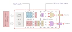
By Dr. RADHA NAGARAJAN, CTO, Inphi Corp. -- The combination of silicon photonics for highly integrated optical components and high-speed silicon complementary metal-oxide semiconductors (CMOS) for signal processing will play an even larger role in the evolution toward low-cost, low-power, switch pluggable optical modules – enabling massive interconnections between today’s vast regional, live data center deployments. The highly integrated silicon photonics chip is at the heart of the pluggable module. Compared to indium phosphide, the silicon CMOS platform enables foundry-level access to optical components at much larger 200-mm and 300-mm wafer sizes. The photodetectors for the 1300-nm and 1500-nm wavelengths are built by adding germanium epitaxy to the standard silicon CMOS platform. Further, silica and silicon nitride-based components may be integrated to fabricate low-index contrast and temperate-insensitive optical components.   In Figure 1, the output optical path of the silicon photonics chip contains a pair of traveling-wave Mach Zehnder modulators (MZM), one for each wavelength. The two wavelength outputs are then combined on-chip using an integrated 2:1 interleaver that functions as the DWDM multiplexer. The same silicon MZM may be used for NRZ and PAM4 modulation formats, with different drive signals.     Figure 1. Silicon photonics enables compact, high-speed optical modules.   As bandwidth demands in data center networks continue to grow, Moore’s Law dictates that advances in switching silicon will enable switch and router platforms to maintain switch chip radix parity while increasing capacities per port. The next-generation of switch chips are all targeting per-port capabilities at 400G. Accordingly, work has begun to ensure optical ecosystem timelines coincide with the availability of next-generation switches and routers.   Toward this end, a project has been initiated in the Optical Internetworking Forum (OIF), termed 400ZR, to standardize next-generation optical DCI modules and create a vendor-diverse optical ecosystem. The concept is similar to WDM PAM4, but scaled up to support 400-Gbps requirements.   2019 is definitely an exciting time for DCI. As we finish the first quarter of 2019, we’re all excited to see what the rest of the year will bring – and look forward to these predictions becoming reality.
www.lightwaveonline.com

By Dr. RADHA NAGARAJAN, CTO, Inphi Corp. -- The combination of silicon photonics for highly integrated optical components and high-speed silicon complementary metal-oxide semiconductors (CMOS) for signal processing will play an [enormous] role in the evolution toward low-cost, low-power, switch pluggable optical modules – enabling massive interconnections between today’s vast regional, live data center deployments.

The highly integrated silicon photonics chip is at the heart of the pluggable module. Compared to indium phosphide, the silicon CMOS platform enables foundry-level access to optical components at much larger 200-mm and 300-mm wafer sizes. The photodetectors for the 1300-nm and 1500-nm wavelengths are built by adding germanium epitaxy to the standard silicon CMOS platform. Further, silica and silicon nitride-based components may be integrated to fabricate low-index contrast and temperate-insensitive optical components.

See Also: Dos and don'ts when working in a data center

In Figure 1, the output optical path of the silicon photonics chip contains a pair of traveling-wave Mach Zehnder modulators (MZM), one for each wavelength. The two wavelength outputs are then combined on-chip using an integrated 2:1 interleaver that functions as the DWDM multiplexer. The same silicon MZM may be used for NRZ and PAM4 modulation formats, with different drive signals.

Figure 1. Silicon photonics enables compact, high-speed optical modules.

As bandwidth demands in data center networks continue to grow, Moore’s Law dictates that advances in switching silicon will enable switch and router platforms to maintain switch chip radix parity while increasing capacities per port. The next-generation of switch chips are all targeting per-port capabilities at 400G. Accordingly, work has begun to ensure optical ecosystem timelines coincide with the availability of next-generation switches and routers.
Toward this end, a project has been initiated in the Optical Internetworking Forum (OIF), termed 400ZR, to standardize next-generation optical DCI modules and create a vendor-diverse optical ecosystem. The concept is similar to WDM PAM4, but scaled up to support 400-Gbps requirements.
2019 is definitely an exciting time for DCI. As we finish the first quarter of 2019, we’re all excited to see what the rest of the year will bring – and look forward to these predictions becoming reality.

Read the full article at Lightwave

Sponsored Recommendations

imVision® - Industry's Leading Automated Infrastructure Management (AIM) Solution

May 29, 2024
It's hard to manage what you can't see. Read more about how you can get visiability into your connected environment.

Global support of Copper networks

May 29, 2024
CommScope designs, manufactures, installs and supports networks around the world. Take a look at CommScope’s copper operations, the products we support, our manufacturing locations...

Adapt to higher fiber counts

May 29, 2024
Learn more on how new innovations help Data Centers adapt to higher fiber counts.

Going the Distance with Copper

May 29, 2024
CommScopes newest SYSTIMAX 2.0 copper solution is ready to run the distanceand then some.